Universal DRSSTC Tesla Coil Driver 2.7 Rev C
The
Universal DRSSTC Driver 2.7 Rev B (Oct 2014) - UD2.7C is the newest
revision.
Here is my take on Steve Ward's Universal DRSSTC Driver 2 which I have
named UD2.7. The UD2 is THE benchmark DRSSTC
Tesla Coil
driver: it has stood the test of time and been used in
thousands of high performance coils around the world. I came across Steve's original UD2 a while
back ago, but there were several new features I wanted to
incorporate. To be very clear, the original UD2 and essentially all of
its design must be credited to Steve Ward - without him there would not
be a UD2! In
addition, I thought it would also be a good idea to share a little bit
about how the UD2 works and how to get one working, with the Tesla Coil
community (with Steve's permission and generosity). Hopefully this
will be a useful resource to hobbyists around the world. The UD2.7 (now in
revision C) has since been
used successfully in a variety of coils, ranging from small table top
400kHz DRSSTCs, 35kHz large DRSSTCs with a full bridge of CM600 IGBTs
and even QCW operation (see application notes below).
This project will not be possible without the work of many people in the
high voltage community. Many thanks to Steve Ward for his generosity in
sharing the UD2 with the Tesla Coil community, and for his permission
for the modification and publication of this new version of the
Universal Driver. The UD2.7 is free for download for personal hobby use;
credit and all rights of the UD2 design goes to Steve Ward. Also, credit
goes to the many improvements made by Bart and Eric in the earlier V2.1
and V2.5 revision, which added many useful features.
At the moment I'm quite happy with the UD2.7C revision, and any new
features will probably be incorporated in a completely new driver design
I am working on for the future. Feel free to drop me a note if you've
successfully used this in your project or if you have any
suggestions or comments!
Quick Links
History and Overview
Theory of Operation
Schematic
Testing and Debugging
Tuning Phase Lead
Setting Over Current Detection
QCW Operation
Downloads
Latest Version V2.7 Rev C (as of Jan 2015)
- Schematic Rev C .png
and board layout .png
- Gerber Files of Rev C ready for production .zip
- Bill of Materials (V2.7 Rev C) .pdf
- Populated Mouser Project
Order
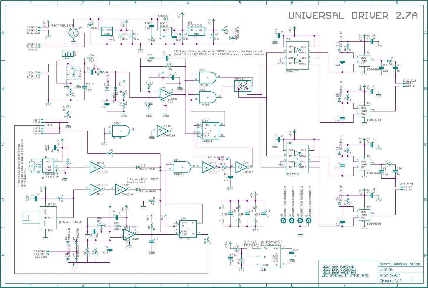
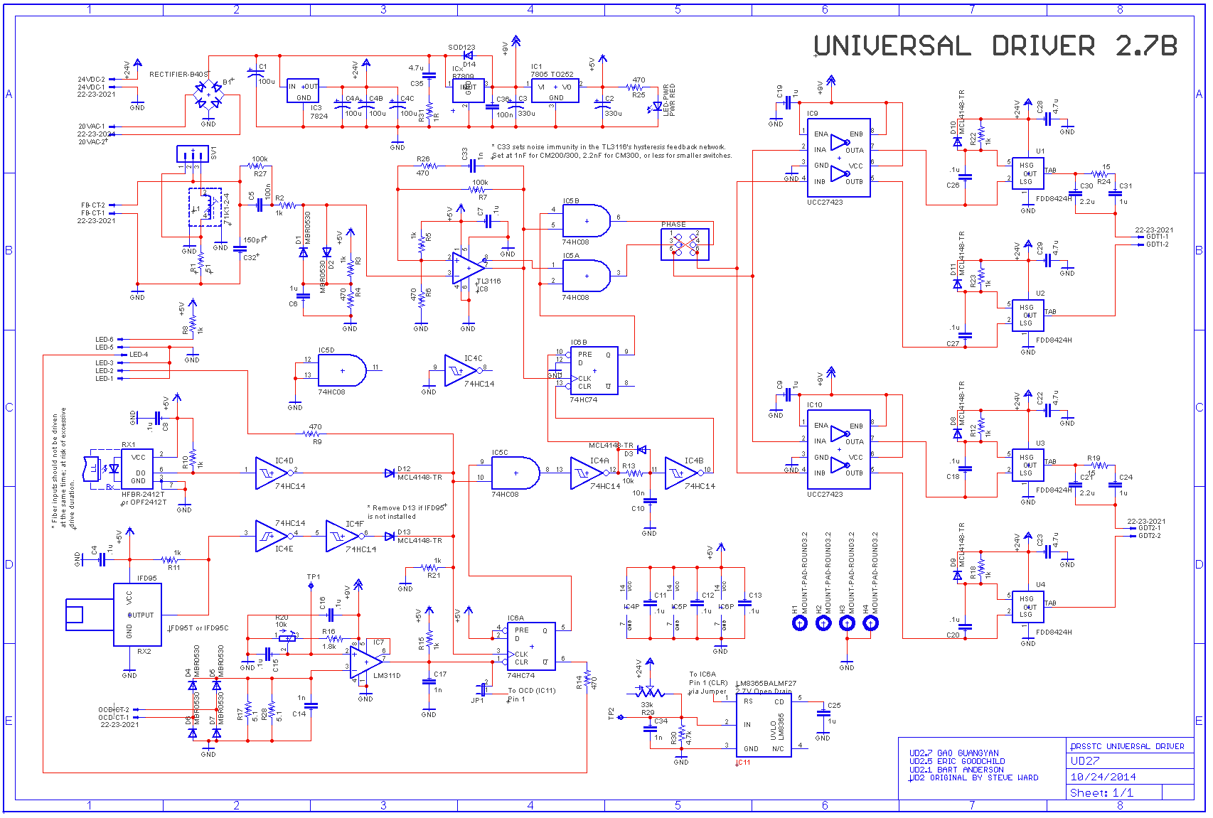
Previous Version V2.7 Rev A/B (not recommended any more)
- Schematic
.png
or .pdf
or .sch
and board .brd
... or UD2.7B schematic .png
- Gerber Files ready for production (V2.7 Rev A, 15
Sept 2014) .rar
See this
4hv forum thread for questions,
discussions and answers. This page will also
be continually updated.
If there are additional changes desired / comments / feedback,
please let me know for a future revision of the board.
Quick Notes
24VDC Input
- Small error in the UD2.7A and B design which has been fixed in the
UD2.7C; also does not apply if you are
only using the AC input jack. Otherwise, there is a simple fix if you are using the
24VDC input jack for the Rev A and B boards: solder on a general purpose diode across the
24V regulator from output to input (i.e. as a reverse protection
diode). See
below for more details.
C33 - C33 sets the dead time for the
TL3116 comparator hysteric feedback network for switching noise
immunity. The pads for the capacitor are increased in size for easy
changing of components. Good values range from
220pF to 2.2nF. For large IGBTs at low switching frequency (e.g.
CM600), use 2.2nF. For medium sized switches like CM200, 1nF
works well (change C33 to less than 1nF for operation above 200kHz). For
faster small IGBTs such as TO247 IGBTs at higher frequencies, use 220pF. Adjust C33 if noise
is found on the output of TL3116.
Fiber Units - The UD2.7 allows the
use of two different kinds of fiber optic input (the ST-type, and Industrial
Fiber Optics type). Use OPF-2412T or HFBR-2412T for ST fiber receivers,
& Industrial Fiber optics IFD95T or IFD95C (these are Active-High, be
careful that you do NOT buy the active low kinds). The fiber units are OR-ed together, so be sure to ONLY use one port for interrupter input to
avoid excessive pulse-widths. They can be installed individually by
themselves to save cost.
D13 - You can install both, only the
ST, or only the IF receiver to save cost. However, because the IF
receivers are active high, if you only install the ST receiver, you must
remove D13 to prevent the interrupter line
from not being pulled low.
Slot-7 Inductors - These 7M3-series
tunable inductors for phase lead adjustment can be bought or sampled
from www.coilcraft.com.
Inductance values varies depending on your switch and switching
frequency. Typical values include: 7M3-123 (9 - 15uH; works well with
TO247 IGBTs), 7M3-153 (11 to 19uH), going up through 7M3-223 (17-28uH),
333 (25-41uH), 393 (29-49uH; works well with CM200/300s), 563 (42 -
70uH) etc. Use a flat-head non-magnetic or plastic screwdriver for
tuning (see instructions below in this page).
Output Drive - UD2.7 has two identical
outputs for driving two bridges (via two GDTs), or can be paralleled to run a
single large
bridge (via one large GDT). To save BOM cost, the second gate drive section can be removed
during assembly -
anything after the phase jumper can be removed for the second circuit,
including the UCC FET drivers and the push-pull MOSFTs.
Feedback - I try to aim for about 1A
of feedback current; adjust your CT turns ratio appropriately. i.e.
if I'm expecting to run my bridge at 500Apk, I'll wind a 500:1 feedback
current transformer.
OCD Burden Resistor - The OCD burden
resistor (R17) is a single 5.1R 2W by default. For flexibility, an
second parallel space at R28 is provided for an optional secondary
resistor. The comparator voltage should ideally be less than 7V to keep
within the bounds of the comparator when on a 9V rail.
Setting OCD Current Limit / Phase lead -
See application notes below.
UVLO Setting (for UD2.7B onwards) - UVLO
trips when the voltage sense line drops below 2.7V (or 4.5V depending on
the part you use). This is set in
UD2.7A with a 33k/4.7k resistor divider across the 24V rail giving about 3V, for
the UVLO to trip when the 24V line drops to 21.65V or so. In
UD2.7B
onwards, R29
is a 50k pot which can be adjusted greater than 33k for a faster trip,
or a less than 33k for more leeway in 24V drop. Tap point 2 (TP2) is
conveniently located near R29 for easy voltage adjustment. This can be
set to 3.0V (or 5.0V for the 4.5V trip).
Note that the maximum voltage the LM8365 can tolerate is 6.5V.
By default, R29 (50k pot) comes set to half (25kR resistance). This
gives a safe voltage of around 3.8V by default which should be adjusted.
However, IF R29 is set to say 0R, this can place a very high voltage
(>6.5V) to the LM8365 causing it to pop! Be careful
when installing R29!
UD2.7 List of Improvements from UD2.0
Change List from UD2.0 to UD2.7A
- Heat-burning 9V regulator replaced with an
efficient switching
regulator (but still TO-220 compatible if you want, with space for heatsink!)
- All other regulators replaced with SMD ones, reducing overall height
of the board
- Added on-board SMD LED for power indication
- Under-voltage Lockout added for the 24V rail with threshold adjustment
- Flattened ground plane and some re-worked traces and component placing
- Added new 24VDC input jack for use with small DC power supply instead
of power transformer
- Improved solder pads for hard-to-solder components such as the dual
MOSFETs and some others
- Added series capacitor with 15R resistor in parallel with 2uF GDT
output capacitor to prevent burning out resistor in event of malfunction
- Improved silkscreen for easier use (e.g. LED breakout jack now labeled
on top)
- All through-hole resistors are now flat instead of standing up, for
increased robustness
- Some components changed to further reduce height of populated board
- Board edges rounded, mounting holes changed to circles, board size
shrunk to be even more compact
- Main component reference IDs (e.g. C33) maintained for easy discussion
on forums
- Includes all improvements from UD2.5 by Eric, such as added IF fiber optic input,
test point for OCD, and fixed errors
- Created BOM, documentation, and improved schematic
- New compact size - 2.4 x 3.7" footprint
More improvements for Rev B & Rev C
- Improved silkscreen and component placing
- Additional optional gate-drive capacitor pads add for use in high duty
cycle
applications with long pulse gate drive durations (optional)
- Added UVLO adjustment potentiometer for lock-out adjustment (or you
can use a resistor instead for a fixed one) and UVLO jumper
- Improved heat-sinking capabilities of 24V and 5V linear regulators
with less thermal relief on polygon pours
- Fixed error on 24VDC rail with now higher AC input range of 19-26.5VAC
nominal and 28VAC max
- Yet more improvements to silkscreen including diode direction labels
and other cosmetic improvements
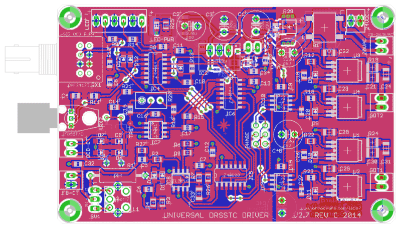
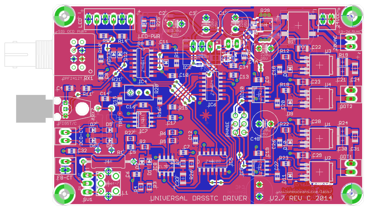
Board layout of UD2.7C showing top traces (red) and bottom (blue) with
silkscreen (white).
For more information / documentation , please read
below.
July 2014
History
What is the UD2? (summary)
The UD2 is a universal DRSSTC driver / controller board
originally designed by Steve Ward, and is an evolution of his UD1.3. The
UD2 accepts a fiber-optic interrupter input
and is capable of driving some large GDTs for DRSSTC operation with a
full or half bridge inverter. Its'
main feature is an adjustable phase-lead controller. It has had a proven
track-record in the field and has been used by many serious hobbyists around the
world.
UD1.3b
Steve Ward created the original Universal DRSSTC Driver
(referred to UD from now on) back in 2008, and was designed to be a
general purpose solution for most conventional DRSSTCs, yet powerful
enough to drive a large full bridge of transistors. It featured the
usual primary feedback circuit with a flip-flop, optical interrupter
input, over-current detection (OCD) as well as robust MOSFET driven
Gate Drive Transformer outputs. Version 1.3b was popularized on his
website and has been successfully used by many hobbyists around the
world.
UD2, 2.1, 2.5
In the quest for a better controller, Finn Hammer came
up with a clever idea of using Phase Lead in his driver; a feature which he called
'Prediktor'. In essence, a little bit of phase lead is added to the
input signal to the driver. The result is that the power transistors can
now be switched slightly earlier - this is desirable because large IGBTs have
a non-zero switching time, and switching earlier allows for perfect zero
voltage switching. Using this idea, Steve Ward
developed a newer controlled dubbed the UD2, adding adjustable lead
compensation via a variable inductor in a LC feedback network. Since
then, several improvements and fixed have been made to the UD2 such as the UD2.1B
by Phillip Slawinski and Bart Anderson, as well as a more recent
improvement the UD2.5 by Eric Goodchild; a shout-out to them for
their work! These improvements have
resulted in additional features such as small fixes, addition of an
additional fiber input, component placing, and other tweaks. Many thanks
and credits to these folks who have contributed back to the Tesla Coil
community.
However, there were still some problems left which I
really wanted to improve and use in my own projects, so I decided to do my
own revision on the UD2. I don't know what the naming convention is but I've
decided to call it UD2.7. I've built on the work
contributed
by the Tesla Coil community, but all rights are still reserved by Steve
Ward who originally created the UD2!
Some of the main problems I had with the UD2
were the linear voltage regulators, especially the 9V and
5V regulators which had a habit of getting very hot with reports
of them letting out their magic smoke due to heat/overvoltage. The
original UD2 placed the regulators in a very awkward position
which was difficult to heat-sink. This was addressed in UD2.5,
but I really wanted to do away with heat sinks for reliable
long-term enclosed operation. In addition, the
UD still did not have a Under-voltage Lockout, which I
think is essential. I also wanted to improve the hand-solderability
of the board, and make the board easier to use.
I made a list of improvements I wanted and
implemented them. The result is what I hope to be a more physically
robust board, as well as a driver that is more reliable for long-term operation in a
confined space.
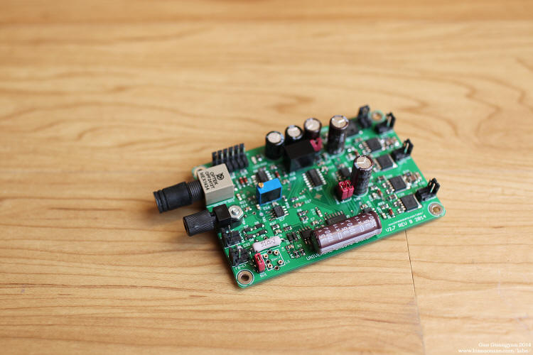
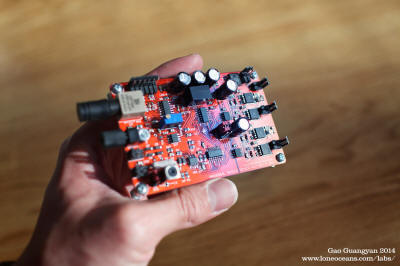
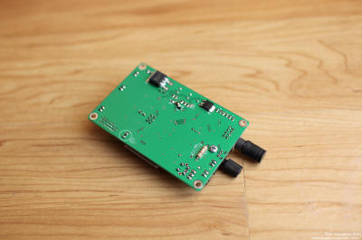
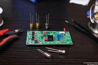
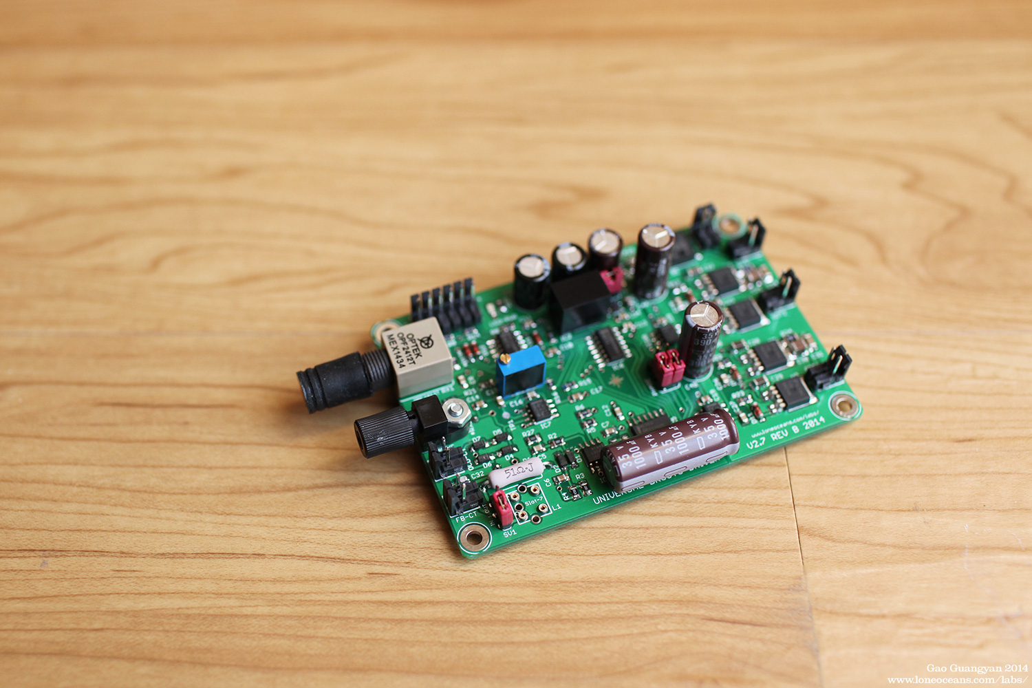
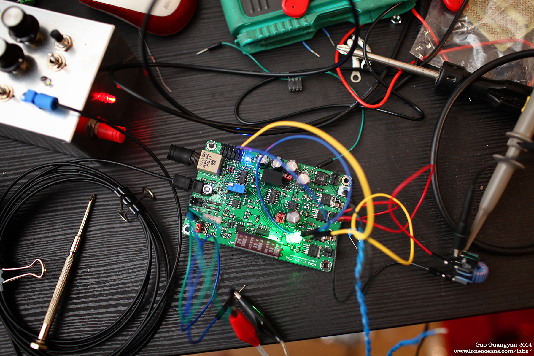
Photos of the UD2.7
These are some photos of the completed and assembled
board. These photos show the UD2.7A.
Notice that I've hidden some components at the bottom
of the board to maintain the general layout and to avoid changing the
size of the PCB.
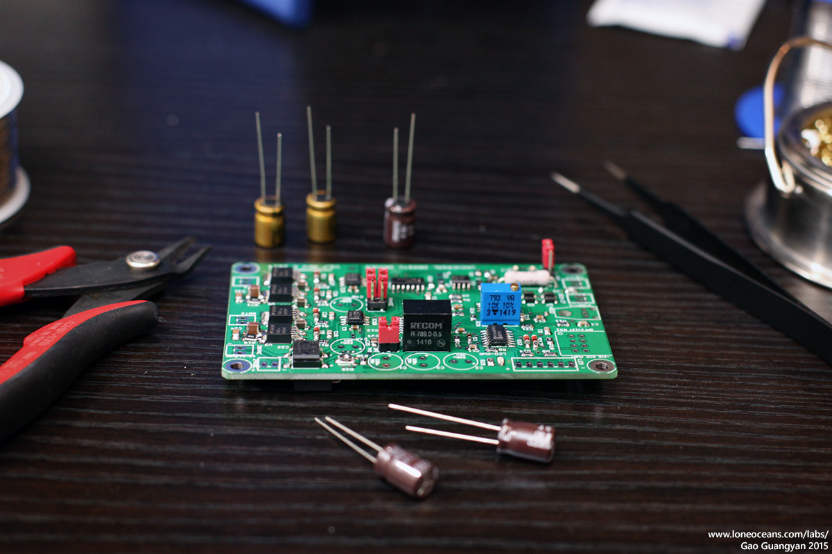
Above in green is a slight revision to the UD2.7A - the UD2.7B. It is essentially identical except for a few tweaks, and
has added space for an optional large drive capacitor (C4C), along with UVLO
adjustment.
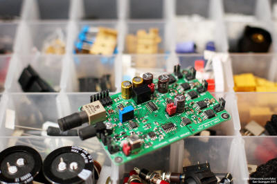
The latest revision is the UD2.7C, hopefully with final
modifications. Above shows a UD2.7C decked out with some shiny gold
capacitors!
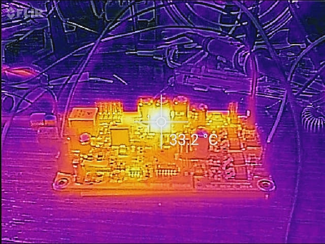
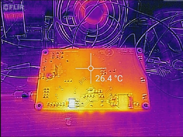
Thermal Analysis
As mentioned, one aspect of previous UDs were that the
linear regulators (especially the 9V one) got really hot. I wasn't keen
of the idea of heat-sinking, so I replaced the regulator with a
switching one, and mounted the other two (changed to the SMT variant) on
the bottom of the board. The large ground plane at the bottom of the
board acts as a heatsink for the regulators.


I used a FLIR thermal camera to see how warm these
components would get when fed with 20VAC, with an ambient temperature of
24C. After 5 minutes of idle time, the hottest parts of the
boards were still the regulators with the 9V switcher topping out around
33+C and the 5V regulator at about 32C. The bridge rectifier and the 3116 were also very slightly warm.
Regardless, a significant improvement over the previous boards which had
regulators that ran
closer to 70C! In typical use, the main regulators and switching FETs
will get a fair bit warmer but still run much cooler than the original
design
.
If you're tinkering with a UD2, you should already be quite
familiar with DRSSTC, have a solid understanding of basic EE, and should be able to figure out
how to read the schematic. I've seen many
beginners wanting to build their first DRSSTC with a UD2 without
prior EE experience. In my opinion, if you are new to DRSSTCs or
SSTCs, I'd highly recommend learning a little more by building a
simpler non-resonant SSTC first, before moving on to DRSSTCs and
the UD2 controller.
General Specifications for UD2.7C
Input - 19 to 26.5VAC recommended input, with
18-28VAC absolute limits. Alternatively, use a 24VDC
input (choose and use one of the appropriate input headers)
Frequency Range - Tested from 12kHz to 1MHz (C33
= 2.2nF from 12kHz to 240kHz, C33 = 220pF to 1nF for up to 1MHz)
Compatible IGBTs - Huge range - from small TO220
IGBTs / MOSFETs to a full bridge of CM600HA IGBTs
Gate Drive - Two push-pull +- 24V
Gate-drive-transformer drivers, can be wired in parallel for
driving larger bridges
Wiring Diagram
The UD2.7 can be wired up as described in this quick set-up
diagram:
Some things to note include:
-
Ability to use either a
24V SMPS or a 18-20VAC transformer. A roughly 30VA power source
should be sufficient for most coils, but you should calculate
the total gate drive power required to be sure. Ensure that you
are plugging the power supply in the correct input jack as
labeled on the board since there is no reverse protection for the DC
input.
-
For CT feedback, I aim for about 1A of feedback;
wind your feedback current transformer to achieve this ratio.
-
OCD trip values work best around 2 to 7V to work
within the range of the comparator. This should dictate what turns
ratio you need for the OCD CT, when combined with the 5.1 ohm burden
resistor.
-
The GDT
outputs can be wired in parallel for driving a large bridge
of IGBTs such as CM600s.
-
Note that the above diagram is of the
UD2.7A. The B revision onwards includes an extra jumper for UVLO,
as well as a potentiometer for adjusting the UVLO set voltage (via
Tap point 2), and extra through-hole pads for C4C, for more 24V rail
capacitance if required.
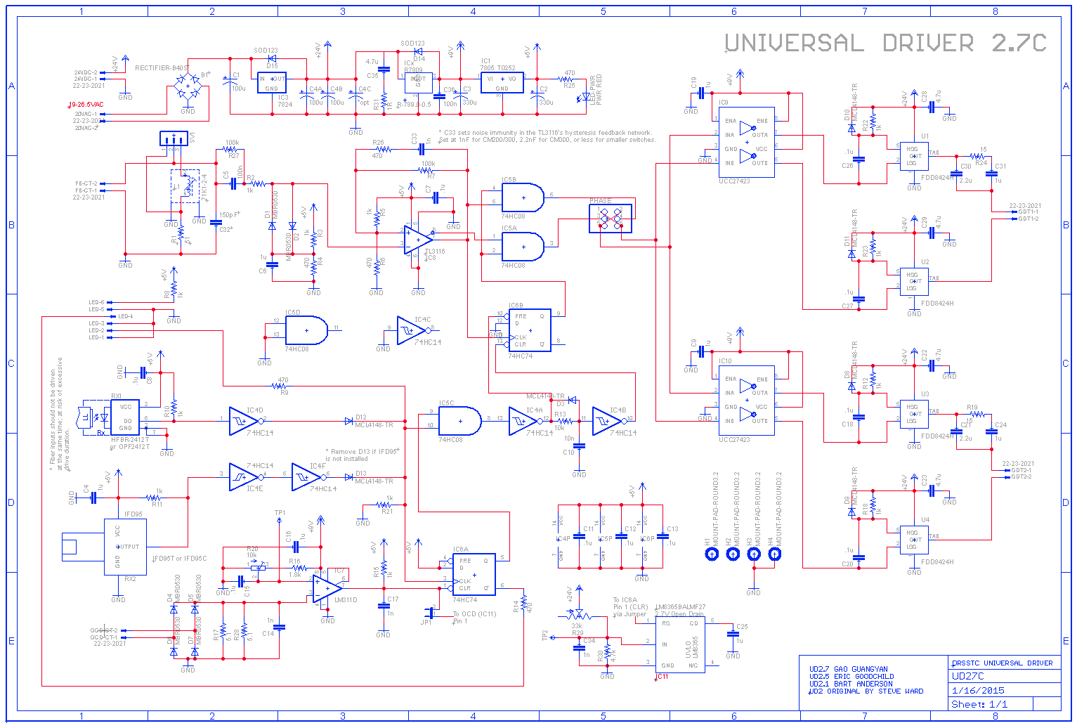
Here is the complete schematic for UD2.7 updated with my
modifications and presented with permission from Steve Ward.
UD 2.7C schematic - click to see in full
resolution.
Let us go through overall the different components of the
circuit. I won't go into them with too much detail, but if you
have any experience with electronics, you should easily be able
to figure out out all by yourself. For previous versions, note that the
Rev B has a few
tiny changes to Rev A.
If you find any mistakes that I have made, please let me
know! [Update - Errata found in the 24VDC input
jack with simple fix - see here
for more details! - this is fixed in Rev C where the 9V
regulator is now daisy-chained off the 24V regulator].
The Gate Driver
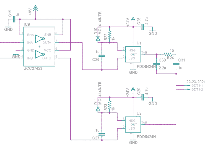
The gate drivers are straightforward and designed to drive Gate
Drive Transformers with 50% duty cycle. I have reproduced one of
the two identical gate drive blocks above for simplicity of
discussion.
Beginning from the left to right, the control signal comes in to
IN_A and IN_B of the
UCC
Inverting Mosfet drivers
(note that the UCCs here are always enabled, and they are dual
inverting). These input control signals come from the logic
section of the UD2, and IN_A is logically opposite of IN_B. You
would think that it is possible to drive a GDT direction from
the outputs of the UCC27423, and you would be right - the
UCC27423 is a dual 4A MOSFET driver, and they are capable of
driving a small GDT by itself, but we can add a complementary
MOSFET buffer on the output of this to beef up the gate drive
capability in both voltage and current.
Instead, the UCC27423 is used to drive the gates of pair of
complementary N/P FET pairs - these are two FDD8424H
40V 20A MOSFETs.
This output stage creates the +-24V signal to the GDT output.
Note that driving your IGBT gates at 24V is
over typical maximum operating characteristics of almost all
IGBTs! There are several reasons for over-driving the
gates though it is not a topic for discussion here. Suffice to
say it is possible to have a lower input on the 24V rail all the
way down to around 11-12VDC as long as it is sufficient for the
9V regulator's input. Adjust the UVLO accordingly if you are
changing the 24V rail voltage. Another alternative is to wind
your GDT with a less than 1:1 turns ratio.
Note that the schematic labeling is a bit confusing here - TAB
corresponds to D1 and D2 of the FET pair in the FDD8424H; S1 is
tied to GND, S2 (of the P Channel FET) is tied to 24V.
Output of the UCC begins as high (9V), turning on the N channel
FET and pulling the output (TAB) to GND. At this time, G2 (pin
5) is pulled by R22 to be 24V, so the P Channel FET is off. When
the UCC begins switching, OUTA/B goes to 0V, turning the N
channel FET off. The signal is capacitatively coupled via C26,
creating a square wave signal same as in the drive signal on pin
2 as pin 5, but shifted by 24V (so about 24V to 15V). The
FDD8424H pair here has a very low gate threshold V_gs voltage of
1.7/-1.6V N/P. This causes the N FET to go OFF, P to go ON,
causing TAB to swing to 24V. Likewise, this happens the same way
on the other pair, creating a 24V push-pull output for the GDT.
The diodes (D10/11) is necessary to clamp the P-FET gate to a
maximum of 24V. Otherwise during the 0V to 9V transition, the
P-gate will jump from 24 to 33V. D10/11 allows current to flow
through during the transitions in on direction, keeping the gate
to a 24-15V drive waveform.
Notice that the output from the push-pull pair is capacitatively coupled via the
DC-blocking capacitor C30, a
beefy high current capable 2.2uF MLCC capacitor. This is important as it prevents
'flux walking' on the GDT and eliminates any DC bias which can
lead to core saturation. R24 is a
15R resistor that damps ringing with the leakage inductance of
the GDT and circuit capacitance, which might accidently turn on
the IGBTs on the GDT secondary. To prevent burning out R24 in
the event of a malfunction (e.g. suppose the driver is stuck on
high and low on both sides for some reason, there will be 24V across the
resistor for a long time which could burn it out), C31 is added
as a DC blocker. This circuit is
duplicated twice for two outputs.
Feedback and notes on over-current setting
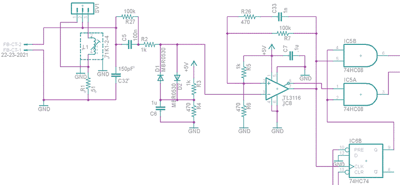
The UD2.7 is simply a current-sending feedback driver at its heart, and feedback
is usually obtained from the primary resonant circuit via a current
transformer. The UD2 adds phase lead functionality, where the
feedback signal is fed into a LR circuit, which adds some
lead-time into the feedback signal, adjustable by the inductance
of L1. We know that across an inductor, the current lags the
voltage (and opposite across a capacitor, where the voltage lags
the current). This is the way phase lead is introduced by the
inductor, where the feedback current is lagging the voltage
signal, and it is this voltage signal we are sending to the
fast TL3116 comparator.
There is some 'cleaning up' after the LR stage before the signal
arrives to the comparator, to square it up as much as possible.
The phase lead voltage signal is sinusoidal in nature, which can
lead to a variable output delay when fed into a comparator with
a wide hysteresis band. As a result, the phase lead circuit uses
a relatively high voltage across the LR filter (~50+V across the
51R at 1A), and then fed through a resistor into a diode clamp
circuit to make it into a reliable square signal. Note that during the beginning
cycles, the feedback voltage starts off
small, so the comparator needs to have a small hysteresis band
to avoid noisy switching, so that the delay between zero
crossing feedback and the comparator output change is small. The
high voltage minimizes this switch delay, especially during
startup.
The current in the CT matches the current in the primary
resonant circuit and is sinusoidal in shape. R3 and R4 together
with C6 acts as a resistor divider from a 5V rail to generate a
DC-offset of about 1.6V. R2 attenuates the signal which is
capacitively coupled via C5, to create a superimposed sinusoidal
feedback signal with a 1.6V voltage off-set. The two diodes D1
and D2 help to 'square up' the signal to form a more
square-shaped, AC signal centered around 1.6V with faster rise
and fall times. This is then fed into IC8, the fast comparator
with a compare reference voltage of 1.6 (formed by R5 and R6),
which places the comparator in its optimal operating range. Note that TL3116
can be replaced with a variety of fast pin-compatible
comparators.
In this way, the TL3116 acts as a zero current crossing detector.
After the comparator is a little bit of simple logic before
going to the gate drive block we discussed previously.
The two outputs of the comparator (inverted and non-inverted) go
into IC5 (AND gates), which then act as the logic signal for the
gate drive block.
The non-inverting output of the comparator also acts as a clock signal to the 74HC74 D Flip flop.
The output of the flip-flop (Q) must be logic 1 for both the AND
gates to send an output to the gate driver. The flip flop therefore
acts as the control to turn on and off the drive, and this can
be achieved by forcing Q to go high or low. We will see how the
interrupter input turns on the drive signal, and this can be
stopped by OCD, end of drive, or UVLO, all synchronized to a
zero-crossing event by the flip-flop (where the output of Q only
changes at the next rising clock edge).
One effect of this is that the flip-flop can only shut off the
drive at rising clock edges, so depending on the phase of your
feedback, it can either shut the drive at n cycles or 0.5+n
cycles. This also means that the current can potentially grow
for about 1.5 half-cycles at worse case, so you need to be aware
of this and set your current limit conservatively.
Here's a back-of-the envelope example: Suppose my primary
current ring up is more-or-less linear and rings up at about
100A every half cycle. I want to make sure my IGBTs see at most
1000A, and this will happen in 5 full cycles. At the worse case,
it takes about 1.5 half cycles to trip the OCD, hence the OCD
should be set at around 850A or so. This will lead to turn off
after a peak current of either 900A or 1000A depending on CT
phase.
Interrupter input and Over-current Detection
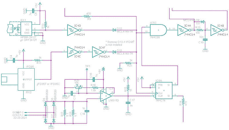
For safety (physical isolation) and noise immunity, control
to the UD2.7 driver is via a 1-bit fiber optic transmission
system. UD2.7 uses
the dual inputs introduced in UD2.5, allowing the use of either ST
Fiber optic or Industrial Fiber plastic fiber optic receivers. These optic
lines are driven by an interrupter of your choice, (light on =
drive on). Because the ST fiber receiver is active low, the output is
inverted once via IC4D. The open collector output of the IF
receiver is cleaned up using two inverters IC4E and 4F. These
two inputs are then ORed together via D13 and D12.
Note that D13 should be removed if the IF receiver is not
installed, and only one of the optical receivers should be driven at any
one time. Notice that the IF-D95OC has a open collector output
and the IF-D95T is a push-pull TTL output. Since they are active
high (unlike the ST receiver which is active low), if these are
not installed, the input line will not be pulled low by the receiver
(due to R11 pulling it high), and the interrupter line will
appear to be constantly high. Hence D13 needs to be removed.
Now lets look at the Over-Current Detector circuit.
Similar to the FB circuit,
OCD feedback is obtained via a current transformer much like the
feedback transformer. The output is full-wave rectified via
D4-D7, and
loaded across R17 (5.1 Ohms). I usually try to wind my CT to get
about 1A across my load resistor, or about 5V across the burden
resistor.
This goes into the LM311 comparator, which compares this voltage
with a threshold voltage that is set by the multi-turn
potentiometer R20 and R16 (voltage diver).
The output of the LM311 feeds into the CLR' of another flip
flop IC6A, to ensure that an OCD trip is independent of phase-lead feedback.
This is ANDed together with the interrupter signal, and goes
through two inverters before going to IC6B, the other flip-flop.
An additional pad for a parallel resistor R28 is added on the
PCB (typically empty), which can be used in the primary currents
are very high and hence it would be convenient to add a parallel
resistor to lower the burden voltage across the CT, instead of
winding a higher-turns-count CT.
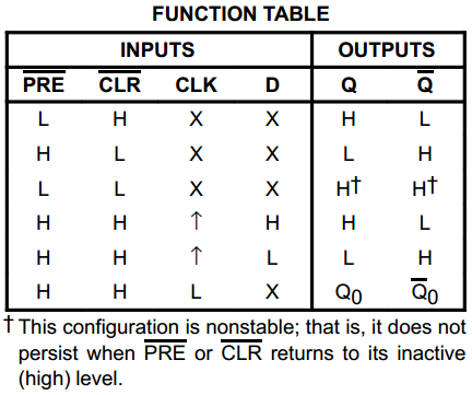
Here's the flip-flop function table (from TI's datasheet):
Now (looking at IC6B), before the OCD trip happens,
PRE' and CLR' are LOW and HIGH respectively, so irrespective of
CLK and D, output Q is HIGH, so our driver is running. So when
an OCD event happens, the output of AND (IC5C) goes to LOW,
hence PRE' of IC6B goes to HIGH a short while before CLR' goes
to LOW because the resistor-cap-diode network R13 and C10 sets a bit of
delay on the order of 100us before the 7414 hits its threshold
HIGH voltage. Therefore IC6B sees HIGH and HIGH on PRE' and
CLR'. Since D is pulled to LOW, on the next rising clock edge
from the feedback, Q is then asserted LOW. If a rising edge
doesn't occur for 100us for some reason, then with H, L on PRE'
and CLR', the drive is shut off anyway. This places a lower
bound of Tesla Coil operation at around 10kHz for ZCS-turn off.
Under-Voltage Lock-Out (UVLO)
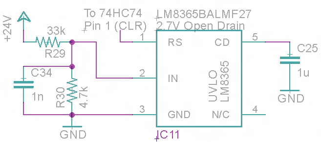
UVLO is straightforward and originally suggested by Hydron from
the forums.
UVLO is an important feature and prevents under-driving of the
IGBT gates if the 24V rail should fall to some low voltage, which
could due to a power loss or a rail sag. Such an event could
also create problems with the logic, so we want to shut down our
drive in such an event. R29 and R30 (replaced by a potentiometer
in B revisions onwards) and form a voltage divider on
the 24V rail such that when it drops to below around 22V, it
will cross the 2.7V (or 4.5V depending on part) threshold of the UVLO IC. C34 is added for
noise immunity but can be omitted. For recovery, C25 sets the
time which is about 1 second before it resets, with 1uF. The
reset (RS) pin is an open drain output and is connected to the LM311
output. As such, it has the same effect as having an OCD event,
pulling P1 of the 74HC74 to 0V, and the drive is shut off at the
next current zero crossing and the OCD LED is turned on, until
the 24V rail recovers and the interrupter is next triggered.
Note that the above schematic is of the UD2.7A. The B revision
onwards includes an extra jumper for UVLO
enable/disable, as well as a potentiometer for adjusting the
UVLO set voltage (via Tap Point 2). For similar operation, set
the potentiometer R29 to be 33k (where TP2 =
3.0V). This voltage can be increased to add
more leeway.
Note that the maximum voltage the LM8365 can tolerate is
6.5V. By default, R29 (50k pot) comes set to half (25kR
resistance). This gives a safe voltage of around 3.8V by default
which should be adjusted. However, IF R29 is set to say 0R by
accident before soldering in, this can place a very high voltage
(>6.5V) to the LM8365 causing it to pop! Be
careful when installing R29! Thanks to Justin on 4hv for
pointing this out!
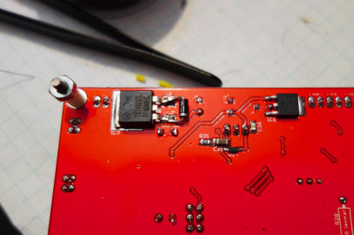
Soldering up the UD2.7
Soldering the UD2.7 should be quite straightforward. I recommend
soldering all the small SMD components before through hole
components. The power Mosfets may be tricky to solder and may
require higher temperature soldering iron to heat up the pads,
as do the voltage regulators on the other side.
Other things to take note are the Polarity of the small SOIC
chips. Also, D13 should be omitted if the black IF fiber optic
is not installed. C33 has larger solder pads for easy changing
of capacitor values. Finally, the right-most two mounting holes
are grounded, while the left-most two are isolated. 4-40
or M3 sized
screws are recommended for mounting the board / IF fiber
receiver.
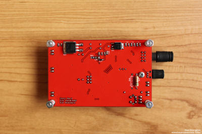
Refer to the photos of the TOP and BOTTOM of the board above to
get a better idea of how the component placing should go. I
found it easier to solder everything SMD on the top side first
before soldering the bottom side, followed by through hole
components.
24VDC Input
Errata for UD2.7A/B [Update: December
2014]
I found a a small error on the PCB (both Rev A and B w.r.t. the
24VDC input) thanks to Daniel, but with a simple fix so no
worries! This only applies if you are using 24VDC input.
This
error has been fixed in the UD2.7C.
Problem: This happens when the 24VDC jack is
used instead of the AC input of only the UD2.7A and B. The 24VDC jack goes directly to
the 24V rail. However, the 9V switching regulator's input is not
connected to the 24V rail but rather the rectified AC rail. I
originally wired it this way to reduce added load on the 24V
regulator, since the 9V switching regulator accepts up to 34V
input. But it looks like I got ahead of myself!
You would think that this meant that the 9V and 5V rails would
not be powered, but it turns out that inside the 24V regulator,
there is a diode in series with about 28k from the output to the
input, hence allowing the regulator to 'conduct backwards'. This
also explains why the board still checked out ok on the voltage
rails, probably helped by the generous amount of logic bus
capacitance and the fact that the logic doesn't draw too much
power. Even without any fix though, the board seems to work fine
powering coils hence explaining why I didn't see the error at
first. However, probably a good idea to fix the problem.
Fix: If you're using AC input, there is no
problem. If you are using DC input there are two ways of fixing
it. First, you can supply 26.5VDC into the AC jack instead - the
diode bridge drops about 0.5V and the 7824 drops about 2V for
24V on the 24V rail. Most 24VDC power supplies usually have
small adjust pot.
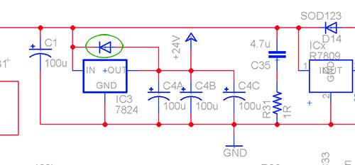
Second way: If you're using the DC input, the problem can be
solved by a simple fix - simply solder on a diode from the
output to the input of the 7824 regulator (i.e. classic reverse
protection diode). So when the 24V rail is powered via DC input,
current flows across the regulator to the input of the 9V
regulator. With this fix, even when powered via AC, the diode is
simply acting as the classic reverse protection diode. The diode
I used for D14 (GSD2004W-E3-08 - just order an extra one when
you're in Mouser) as a reverse protection diode across the 9V
switching regulator can be used for the 24V regulator, or any
other general purpose diode will be fine. This can be soldered
directly across the legs of the 7824 regulator and fits
perfectly. Make sure the diode is from the output to the input.
Above is a fix with a standard 1N4001 diode across the 24V
regulator, on the V2.7A board. In the new V2.7 Rev C, I have
fixed this error and the 9V regulator input is now powered from
the 24V rail.
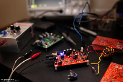
The UD2.7 is best tested with a current limited adjustable power
supply at 24VDC into the DC input jack. Upon turning it on, the
on-board SMD power indicator LED should turn on. At this point,
check the three power rails to ensure that you have 24V, 9V and
5V. None of the components should get warm at all. Next, connect
your fiber optic cable to the fiber optic interrupter of your
choice. Attach a LED on the Signal LED jack (the middle pins of
the 6-pin LED jack). Check that when the interrupter is running,
the LED should light up correspondingly. This verifies your
optical receiver is working. Take note that D13 must be removed
if the IF fiber receiver is NOT installed.
A quick way to verify that the board is working is using a
signal generator running at your desired frequency to simulate
feedback. Set your frequency / signal generator as a sine wave
of around 5V amplitude at your desired frequency (e.g. 100kHz).
Connect this to the input of the Feedback jack (not the OCD
jack). Now connect the ground of your oscilloscope to the ground
of the board and scope the outputs of the gate drive, and turn
on your interrupter.
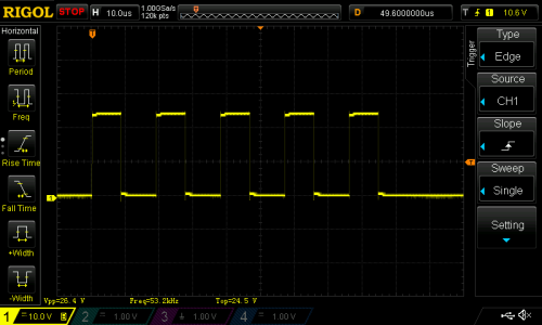
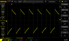
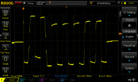
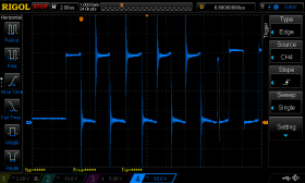
You should see the above 50% duty cycle square wave at +24V at
the input frequency of your signal generator. The example above
shows one of the GDT outputs running at about 53kHz at a pulse width of about 85us.
Because the UD2.7 implements a flip-flop for zero-crossing
turn-off, the gate drive should
always end at a transition point. The amplitude should be
single-sided 24VDC with a 50% duty cycle. If you see this for
all four GDT output pins, your driver is working as expected.
With NO GDT connected, the driver should be quiet.
The driver creates a +- 24V output for the gate drive
transformer. To verify this, I made a very quick lash-up
transformer for test. Note that this is NOT an ideal GDT -
please wind a better one for your own DRSSTC (these scope shots
show too low primary inductance - can be solved by adding
more turns, but this was just a quick lash-up to show the driver
working). Above shows the secondary of the GDT across a small
resistor at 50kHz and 500khz. The photo on the rightmost shows a
situation caused by an incorrect C33.
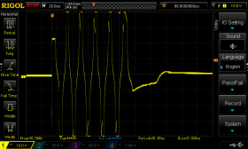
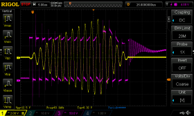
Note that if you have no input signal in your FB jacks, the
driver will not see any feedback, causing the drive to lock up.
Here's a scope shot of a GDT output with a feedback input signal
(left). But if you have a GDT attached with no
signal generator input on the feedback, this will make a signal
on the output of the GDT look like the above (right - where the
driver doesn't know what to do), and will cause quite a loud
audible buzz from the GDT with this associated output per pulse.
This sound should diminish greatly with a feedback input signal.
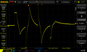
At low frequencies, you might notice your GDT saturating. This
will cause very unstable, ugly switching, and the result will
also be a very erratic and audible buzz on your GDT, as shown in
the three scope shots above. Fix this by making a better
GDT.
You should adjust C33 to suit your
needs. For example, the use of 2.2nF for C33 limits the maximum
frequency to at most ~250khz, resulting in a bad drive (right most
image). If you see this, change C33 to a smaller value (220pF to
1nF), or reduce your frequency. Note that the output is +-24V.
At this point, your driver should be ready for basic operation.
I have tested the UD2.7 all the way from 12kHz to 1.04MHz
(whereas 220pF seems to be good from ~150khz upwards). 1nF
should be good for most applications.
It is also a good idea to test the under-voltage
lockout and OCD. To test the UVLO, continue scoping the output
with the interrupter on, and slowly turn down the voltage from
your adjustable DC power supply. Depending on the tolerances of
your voltage divider on the UVLO, the output of the driver
should stop once it drops below around 22V and the OCD light
will remain on. The minimum lock-out will be about one second
or so, before coming on again when the 24V rail recovers (can be changed by adjusting the
value of the 1uF capacitor). OCD is tested the same way by
increasing an input sine-wave voltage until the set level. At
this point, the OCD light should turn on and the output will
stop.
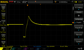
Phase lead can be adjusted by choosing an appropriate adjustable
inductor and carefully adjusting it to suit your Tesla Coil.
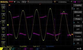
This is the way I usually tune my coils for phase lead. First
determine the general operating frequency of your DRSSTC. In the
example shown in the scope shots above, I am running my DRSSTC
at about 380kHz. Run the DRSSTC without the secondary coil in
place. I usually use a metal object as a load in the middle of
the primary coil. This could be as simple as a metal pan with
some water inside, or a block of steel.
Next, power your DRSSTC as usual, but with a lower bus voltage
if desired. Note that to take scope measurements, you should
isolate your entire drive circuit! This is very important. In
the example above, I am running my bridge at about 170V bus. The
blue trace shows the Collector-Emitter voltage of one side of
the bridge showing the output of the bridge with no
phase lead (this can be set by the jumper beside the
tunable inductor). Note the huge spikes during the transitions
greater than 100V! These can kill IGBTs since IGBTs are
extremely sensitive to over-voltage, and it is very difficult to
get rid of these spikes even with a low inductance layout due to
the intrinsic component inductance which cannot be removed.
I then tried a few different inductors (see quick notes above
for which values to use), and adjusted the phase lead while
looking at the scope. As you move closer to the sweet spot, you
will notice the spikes dropping in amplitude all the way until
they.. suddenly disappear. This is the sweet spot and your coil
is tuned appropriately.
It will be impossible to completely eliminate all switching
spikes. What I do is to ring up the primary (by adjusting the
pulse width on my interrupter) until it hits a current I plan to
run the coil at. In scope shot 2, you can see the primary
current (yellow) versus the bridge output (pink) with
phase lead. At this point, the current ramps up to
about 130A. I have also adjusted the phase lead such that the
spikes are the smallest at the last few cycles when the current
is the highest. The third scope shot shows a close up of shot 2,
showing beautiful, clean switching.
This point is achieved at a type of switching known as
zero voltage switching (ZVS). In this case, the IGBTs
are switching not at exactly at zero current, but at zero
voltage. The best way to visualize this is to overlay the
gate-emitter and collector-emitter voltage of one of the IGBTs
during operation. What you want to see is when the opposing
IGBT turns OFF, the bridge voltage begins to fall to 0 and
invert. Note that IGBTs really turn into a conductive state as
the gate voltage reaches a plateau around 10V. So when scoping
the gate voltage, you will see it rise up quite fast, plateau at
~10V, before shooting up to 24V of the gate drive. The trick is
to adjust phase lead such that just when the bridge voltage
transitions at 0V, the gate is at this plateau, and all ringing
should disappear. For more details, scope shots and tips on
choosing a suitable gate resistor, see my
DRSSTC 3 page where I walk through this procedure in detail.
In summary - set your bridge for ZVS which will lead to the
smallest spikes. Aim for the cleanest transitions at the highest
current. I found that setting for a clean transition at about 20
to 25% of expected peak current usually leads to good results.
Setting OCD on the UD2.7 is as simple as adjusting the large
variable resistor R20, and measuring the
voltage at tap point 1 TP1.
For example, lets say we are building a DRSSTC where we do not
want the IGBTs to see more than 700A primary current. Note that
by design, the UD2.7 only switches the transistors OFF during a
zero current crossing via a flip-flop (this is to prevent
switching off the IGBTs when huge currents are flowing). This
means that even after the OCD trips (say while the current is
ramping up during a quarter RF cycle), the current can continue
rising to higher than the OCD trip point for up to 1.5 half
cycles before it goes back
down. Therefore, we might want to set our OCD point to 600A or
so.
Next, count the number of turns on your primary current
transformer. Lets say we have a 625:1 current transformer made
by cascading two 25:1 transformers. Therefore if 650A is flowing
in the primary, we will see 1.04A in the OCD CT. This current is
full wave rectified and flows across the burden resistor R17
(5.1 ohms). By ohms law, at maximum current, we will see 5.1 x
1.04 = 5.304V across R17. Therefore, adjust R20 until TP1 shows
about 5.3V and you're all set!
Note that for larger coils running at say 2000A with a 1000:1
current transformer, another burden resistor can be placed
along-side R17 (R28), to reduce the burden resistance. Note that
the comparator LM311 has limits at its 9V VCC voltage (minus
some since comparators are not accurate near the rails), so make
sure the trip voltage is less than say 8V or so.
The UD2.7A has been tested to work extremely well in QCW DRSSTC
operation. See my QCW 1 page to see it in
action. However, it was certainly not designed with QCW
operation and therefore you should understand its limitations
which is out of scope for this page and obvious to the skilled
coiler.
Some modifications should be made to the board for proper
operation. This mostly relates to the long drive required by QCW
operation, where the driver has to switch IGBTs for several
thousands of cycles instead of around 10 or so in normal DRSSTC
operation. The result is that the 24V voltage rail may drop to a
dangerously low level due to insufficient 24V rail capacitance
and / or insufficient logic power from say a 20VAC transformer.
Fortunately, the UD2.7A has an under-voltage lock-out, which
will prevent your IGBTs from desaturating and blowing up when
the 24V rail drops too low. However, it might
limit the pulse width you can drive your IGBTs. In addition,
QCWs usually operate at around 300 to 400kHz, and correct
selection of C33 is required.
-
I found using C33 = 220pF works great for high
frequency operation. Solder 220pF
on C33 for 300 - 400+kHz operation.
-
Add extra bus capacitance on the 24V rail. You can
simply replace C4A and C4B with higher capacitance electrolytic
capacitors, or tack on a few extra outside the board. The default
values for C4A/B at 8mm diameter 35VDC 220uF capacitors. I found
adding an extra 1000-5600uF capacitor works great depending on your
application. There is space on the
UD2.7B/C board just for purposes like this (C4C).
-
Iron transformers are usually unable to supply
enough power to the board for QCW operation. Another alternative
instead of adding extra capacitance on board that works great is to
use a 24V
switch mode power supply as a power source (instead of a 20V
transformer). These supplies usually
have an output filter capacitor as well which gives extra bus
capacitance.
You may find that the 24V rail voltage can still drop to 22V,
triggering the UVLO. Another way to fix this is to simply lower
the UVLO trip voltage by lowering the resistance of R29. This can
be easily done by kludging another SMD resistor (say several
hundred kOhm) over R29 in parallel with the existing 33k
resistor. The UVLO IC can be left-out all together, but I do not
recommend this. Your IGBTs will explode if they desaturate with
several hundred amps through them. UD2.7 Rev B and Rev C replaces
R29 with a 50k potentiometer for easy adjusting of the UVLO voltage
threshold.
Back to main page
(c) Gao Guangyan 2016 - 2025
Contact: loneoceans [at] gmail [dot] com |


