A simple, robust and powerful flyback
driver with over-current protection
Half-bridge Flyback Driver
Creating high voltage electrical sparks with a television flyback
transformer is a fun beginner project for many electronics hobbyists. In fact,
the first few HV projects I ever worked on were flyback-drivers of
different sorts (outlined in this page here) -
their simplicity and ease of construction makes them great introductory
projects into the world of high voltage electronics. Common flyback driver designs include the popular single transistor driver, as well as the
ubiquitous and powerful Mazili ZVS flyback driver. Kits based on those
two designs are widely available on the internet and on eBay.
However, I wanted a driver which was even more robust, and capable of driving flyback transformers at
high power levels, yet still being reasonably straightforward to
construct.
This page outlines the design and operation of a half-bridge flyback
driver, and describes how you can build one yourself too!
If you are unfamiliar with flyback transformers and what they
are and how they work, please feel free to read my earlier page on this topic
here, where I describe their method of
operation in detail. This page will focus primarily on the design
and construction of a half-bridge flyback driver.
The completed flyback driver
(with a conservative current limit and driven with 36V on the bus) was
tested up to a measured 120W input power for extended (many minutes) of
continuous run time and remained all cool to the touch. I have no doubt
this driver will do just as well as a few hundred watts - more to come
soon!
For result, please scroll down to the bottom of this page. Thanks for
reading and please be safe if you are attempting the project described here!
Sept 2017
Design and Operation
Overall Project Goals
For this project, I create a few goals:
- Develop a robust and reasonably powerful flyback driver
- Design a circuit which is simple and easy to build, and easy for hobbyists
to replicate
- Be flexible for driving a variety of Television and CRT flyback transformers
- Have some basic over-current protection for reliability
Electrical Design
Based on the above guiding principles, I adopted a half-bridge
driver topology driven by a fixed frequency oscillator.
I could have gone for a more powerful full-bridge inverter, but using a
half bridge saves components and should be sufficiently powerful enough. In addition,
I decided to go with all discrete components (i.e. not using any
programmable ICs) such that hobbyists can easily replicate this project.
Finally, I also wanted some sort of basic protection for overall
longevity and robustness of the system, therefore I implemented a
simple over-current detection which cuts off power when a threshold current is
exceeded.
Ironically, despite the fact that this half-bridge driver
will be driving a flyback transformer, it will not actually drive it
in typical 'flyback - mode'. Instead, this driver topology will operate more akin to a regular, albeit
high frequency, transformer. Specifically, 'flyback-mode'
operation refers to a switching topology whereby the
primary and secondary conduction cycles are non-overlapping. In the flyback
mode, the primary coil essentially acts as an inductor, where energy
from a primary cycle is stored in the magnetizing inductance of the
inductor, and then released to the secondary coil. Driving
the transformer in the manner described on this page therefore is not a typical 'flyback-mode'
drive. However, it still achieves our goal of producing nice arcs from a
flyback transformer.
One popular feature which people may be interested in, is
to create a 'singing' arc. In those instances, the driver modulates power into the flyback transformer based on an audio input. I decided to omit this
feature from this particular project, focusing instead on simplicity. However I do plan to create a much more advanced driver in
the future with this capability (and more!).
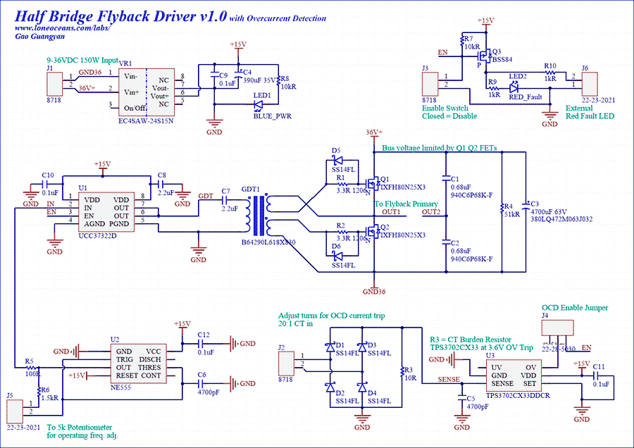
How The Driver Works
Here is a schematic for the completed Half Bridge
Flyback Driver:
The Halfbridge Flyback driver system including design, schematics and
layout are available for use under the
Creative
Commons License.
This is how my flyback driver works.
Power is supplied via J1 which, in this
specific design, can range from 9 to 36VDC. This is the main power supply for the
half-bridge inverter, and also powers the voltage regulator generating
the 15VDC rail which is used for the other parts of the circuit. Note
that the range of 9 to 36VDC is simply the input voltage range to the
small DC/DC converter (VR1) - you could certainly run the driver at even
higher voltages, limited by your main switching MOSFETs, but then you
will have to find another way to generate the 15V rail for the 555
oscillator and gate drive.
Note: To generate the 15V rail, I'm using an
off-the-shelf 5W
DC/DC converter.
You can also replace this with a standard
7815
(TO-220) voltage regulator. However those typically have a maximum 35VDC
input and will get very warm with >20V in (heatsink required). The 7815 also has a 2V
voltage drop at 1A I_fwd, so you will be limited to ~17 to 35VDC input.
For ultimate flexibility from the main bus, the 15V rail can instead be
generated from another external power supply.
Next, a generic 555 timer (U2) is configured in the standard astable oscillation mode with a duty cycle fixed at 50%. The operation
frequency is set by R6 and C6, as well as an external series potentiometer
(5kR), connected to J5. In the schematic above, this
allows setting an operating frequency between about 23.4kHz and
101.3kHz. This square wave is fed into the input of the UCC37322 (U1),
which is a powerful 9A MOSFET driver.
Note: As shown in my schematic above, the 555
generated frequency can be calculated as freq = 1
/ (1.4 * (R6 + J5)*C6 ) where R6 = 1.5kR
and J5 = the value set by the potentiometer and C6 = 4700pF. Another
example is using the same 5kR potentiometer together with C6 = 3.3nF, R6 = 2.7kR, giving us
80.2kHz (when the pot is 0 ohms) to 28.1kHz (5k ohms) operation - I use
these values in my final build. Care needs to be taken such that the GDT
does not saturate at the lowest operating frequency.
Instead of driving a FET directly, the UCC37322 FET
Driver drives a hand-made Gate Drive Transformer, which then drives the
gates of two power MOSFETs. Using a 1:1.6:1.6 turns ratio (for example 10 primary turns and 16 of each secondary turns), this
generates a +-12V gate drive signal across the gates of the power
MOSFETs (from the +15 to 0V across the primary winding of the GDT). Please
read below to see how I made my GDT and what cores you can use.
The maximum input to the half bridge is limited mostly
by the choice of MOSFET used. For example if the popular and cheap
IRFP260 MOSFET is used, something up to ~150VDC can be used. In my case,
I've opted for a more expensive but better MOSFET (IXFH80N25X3 250V 80A)
which should be good for up to ~180VDC or so (though in practice 36V will
produce good results, and is already more than likely to be able to fry
most flybacks!).
Likewise, the DC power supply used needs to be sized
accordingly. I've opted to use a 150W 36VDC DC power supply for this
project which should be more than enough for most applications.
Over Current Detection
A simple over-current-detection (OCD) scheme was also
implemented. This is described in the bottom-right block in the
schematic above, and can also be omitted if you do not want over-current
protection. J4 allows keeping the OCD circuit in system or out of
system.
To achieve OCD, a home-made current transformer (CT) was
created which senses the half bridge output current. This was
constructed using a 20:1 turn ratio CT. The signal from this CT is
rectified through a bridge rectifier (made from diodes D1-4), and
burdened by load resistor R3. The voltage across this is sensed via a
Overvoltage Monitor IC (TPS3702CX33DDCR), which is essentially an
integrated comparator. In this case, the trip voltage for my particular
choice of IC is 3.60V. When the voltage across the burden resistor
exceeds 3.6V, the TPS3702 IC's OV (over voltage) pin is pulled low
(open drain).
As a result, with the current setup, the peak current
limit is set conservatively at 7.2A. To increase the current
limit, either increase the number of turns on the CT, or decrease the
resistance of the burden resistor. For the record for this particular IC, the
propagation delay for an over-volt event is 35us, and the time for
re-enabling is 19us when the voltage falls below threshold. Hysteresis
is 0.55% for the X part I used, with OV thresholds 3.60V and 3.43V.
Having such a low current rating is a little
conservative, but together with our 80A MOSFETs, we should hopefully see
extremely rugged operation and it should be pretty hard to blow up this
driver (touch wood!).
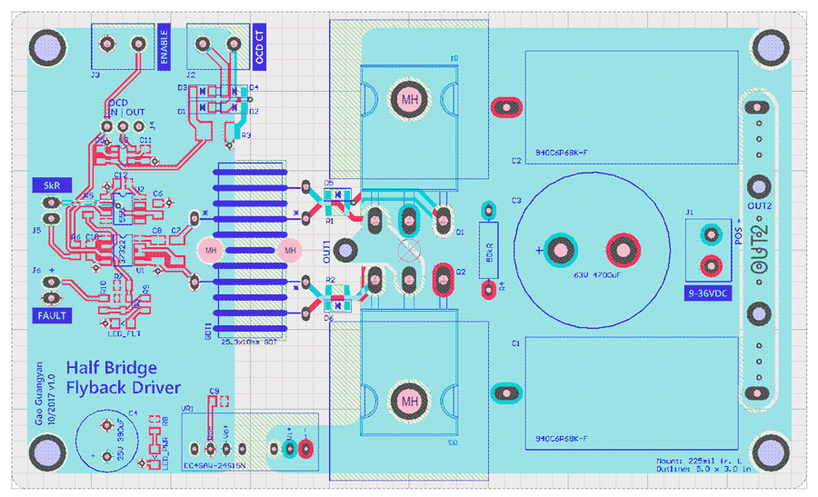
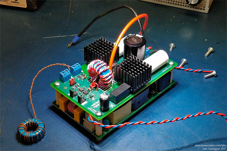
Board Layout
With the design complete, I decided to do a quick lunch-time layout. One thing I thought I wanted to do was to fit everything
into a standard ATX computer power supply box. I decided to go with a
36VDC 150W DC/DC switching power supply as my main power source, and I managed to find one which
had a 5x3" footprint. In order to make mounting easier, I used the
same footprint as the basis for the board layout so I could mount
everything into the box in a tidy way (on top of each other).
After about an hour or two of layout, I got something I
was quite happy with. 5x3" is a lot of board real-estate so layout was
no problem at all. The 36V rail features a laminated bus structure to
reduce switching spikes by keeping the power loop inductances low.
The main power input (from the 36V DC power supply) comes in from the
right into the 5mm screw terminals (J1).
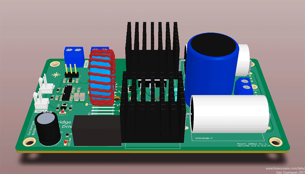
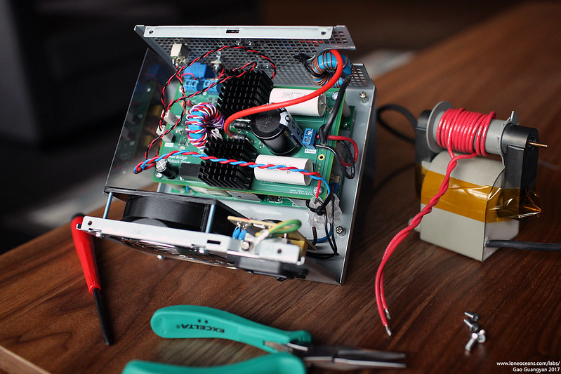
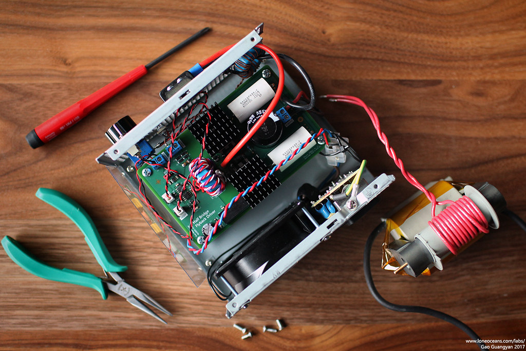
This is how it looks like in 3D. Most computer ATX power
supply boxes come conveniently with a power switch, IEC input jack, and
a 12VDC fan. However we will not have any 12VDC supplies, so I replaced
it with a 80mm AC fan connected directly to mains instead. This fan was
subsequently changed out for a 12VDC fan powered by a 36 to 12V 1A small
switching regulator, thus allowing true universal input operation for
the entire unit.
This fan will provide
cooling for both the power supply and switching MOSFETs which have their
own direct-mount heatsink. Having separate heat-sinks allows for a
direct thermal contact to the transistor package casing and should
improve thermal performance (though probably unnecessary). Not pictured here (or on board) is the
current transformer used for over-current-detection. The Gate Drive
Transformer is a self-wound GDT and cable-tied to the PCB via the 2
drilled holes.
Construction
Putting the Half-bridge Driver Together
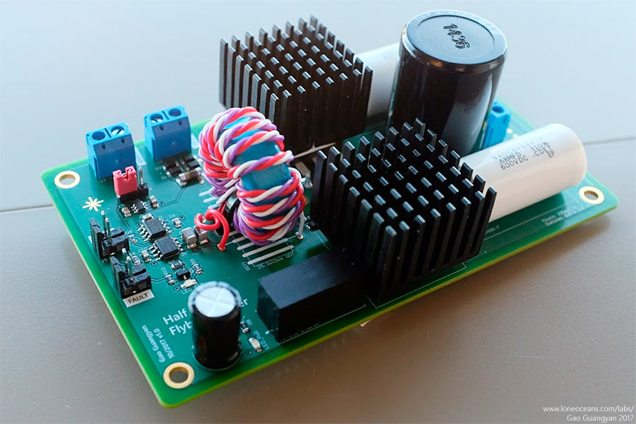
After waiting for a while for the PCB and components to arrive,
I was able to assemble the board together.
There are not too many components so the driver was
assembled fairly quickly. The two things that I had to do an extra
little bit of work was to tap and drill holes in the two heat-sinks for
the transistors - (these are very cheap 28 x 28 x 20mm square heatsinks
from Aliexpress / Ebay), as well as to wind my own GDT.
For those not familiar with GDTs, GDTs are transformers
which allow generating isolated gate drive signals without requiring
isolated power supplies. They work great in this half-bridge design
whereby the first of the secondary winding drives the lower FET and the
second secondary winding drives the gate of the upper FET. In order to
generate the +-12V desired, I opted for a 12:20:20 primary:sec:sec
ratio.
The primary is driving at +15V to 0V, and with the 12:20
ratio should give us +-12.5V on the secondaries. It is critical to make sure that the
GDT core does not
saturate, especially when switching at low frequencies. I opted for a
decent sized 1" diameter ferrite core (N30
material toroid made by Epcos / TDK and commonly found on Mouser or
Digikey), and I twisted 3 strands of wire together (to reduce leakage
inductance). 12 turns were wrapped around the core, then an additional 8
more for the secondary windings.
Care was also taken to ensure that the polarity of the
secondary coils were soldered in opposition (so we only have one transistor
on at any time otherwise a dangerous shoot-through occurs when both
transistors turn on at the same time!). I highly recommend verifying the
polarity with an oscilloscope if you have the slightest doubt since this
mistake will blow your board and transistors up.
Likewise, the current transformer (pictured above made with
brown wire) was wound using the same ferrite core as the GDT. 20 turns were wound on
it. The number of turns can be changed in conjunction with the burden
resistor to change the desired trip current. With the board assembled,
it was then mounted on stand-offs on top of a 36V 150W AC to DC
universal voltage power
supply. Notice how I designed the PCB to fit perfectly on top.
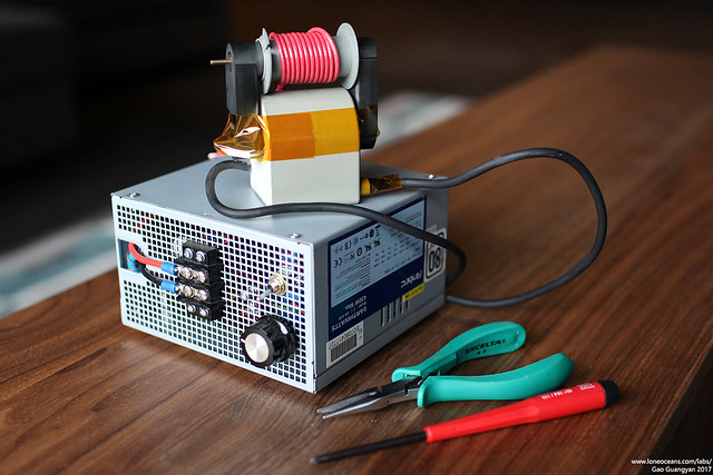
Finally, I placed all the components into a scrapped ATX
power supply case. The case is ideal for projects like these because of
their compact size, essentially no cost, and comes with a built in fan (I
replaced it with a AC fan driven directly from the mains), switch and AC
filtering, power receptacle, as well as a cable hole at the front! All
that was required was for me to drill 4 holes into the bottom of the
case.
A barrier block was mounted at the front of the case, as well as the
enable/disable switch, a bright red LED, and the frequency control knob.
The driver is complete!
Choosing a flyback transformer
To test out the driver, I need a flyback transformer. But what
specific transformer should I use? There are many kinds of flyback transformers. As
described in my flyback page, most
hobbyists prefer the 'wide' or 'fat' secondary winding kinds, as
opposed to the more cylindrical ones. I had a few on hand, but I
also picked up a custom made flyback back in 2014...
In 2014, a forum member on the 4HV forums (Fiddy) made a
custom order of a few transformers. Specifically, and quoting Fiddy,
these flyback were constructed as follows:
• No diodes for true ac output.
• No primary coils at all.
• Insulating bobbin on-core for your own primary
• Large gap between secondary and primary for your own primary winding.
• 3000 turns of 28AWG secondary
• Potted and insulated secondary
• Thin plastic film between core joints
I bought myself one! For reference, above is a photo of
the Fiddy's Flyback (middle) with a F0241 flyback on the left and a
KFS230867 (replaces Koyod HR 42020) transformer on the right which are
traditional CRT flyback transformers. I did a
quick weigh in and they weighed 352g, 668g (with the wire) and 140g from
left to right!
With the much nice construction (and lack of other
secondary windings), this large flyback will be my main flyback of
choice.
Results
Nov 2017
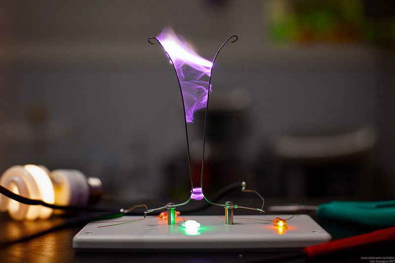
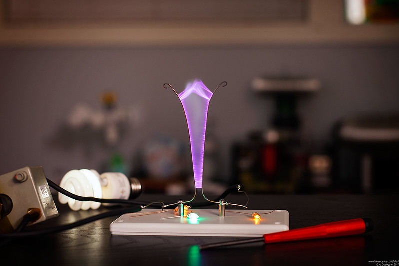
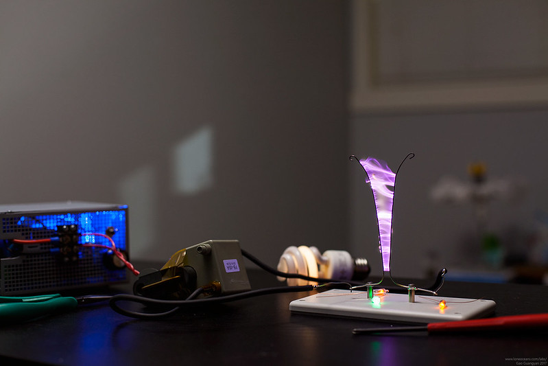
Preliminary Test - mini Jacob's Ladder
I plugged the driver in and it worked first time around,
both with regular flyback transformers as well as with the large custom
flyback! Here are some preliminary results.
For this
first test, I created a very simple Jacob's Ladder out of two
wires and hooked it up to a flyback transformer connected to the
half bridge driver. The driver was fed with 34VDC, which drives
a 12 turn primary coil on the flyback transformer. The result
was some very beautiful arcs ranging from white hot (~30kHz), to
beautiful long purple arcs (~42kHz with some resonant action
going on).
Due to the high operating frequency, the arc is very
quiet and flame-like, dancing between the two wires in a mesmerizing
way.
In this preliminary test, the results were very good.
The half bridge driver performed well showing really no signs of much
heating at all despite a continuous run of around five minutes. The
flyback transformer (windings and core) remained cool as well, with most
of the heat being from the ladder itself. Power level was measured
around 2A at 34V for a roughly 70W operation when arcs are drawn.
Finally, I played around with various settings and drove
this (and other) transformers with varying turns on the primary side
(ensuring the cores do not saturate), and also did some power
measurements. The OCD kicks in perfectly well, and when heavy arcs are
drawn, the TPS3702 (with an at-best 18kHz propagation repetition frequency) comes into
play and limits the current, often with an associated high squeal at the
on-off OCD Frequency! Maximum power measured by a Kill-a-Watt into the
arc (already excluding gate-drive and fan cooling) was measured at max
to be about 120W when drawing hot 2" fiery arcs with no apparent heating
of the flyback transformer or bridge. This is well within the 150W limit
of the power supply and this should all make for very reliable
operation!
As usual, more to come soon and hopefully with much more
power! Need a beefier power supply!
Links and References
Here are a list of links to other great
hobbyists whose work I have learned from in creating this
project. Many thanks to them for pioneering the way!
Thanks to Fiddy on the 4hv forum for making a run
of nice
flyback transformers a while back in 2014 (infosheet)
Other links on 4hv forums include driving flybacks in
flyback-mode,
Marko has a good write-up of a half bridge flyback driver
powered by a SG3525 PWM IC
Steven Ward built a simple and effective half bridge flyback
driver powered by a 555 timer as well
Uzzors2k also builds a 555 timer based flyback driver running in
flyback-mode, as well as other great push-pull drivers
Adam built a nice fat 'Fryback'
transformer, certainly a big thumbs up for construction effort
Advanced Linear Designs has a
concise page
on 555 astable 50% duty operation
Back to main page
(c) Gao Guangyan 2025
Contact: loneoceans [at] gmail [dot] com
Loneoceans Laboratories. Copyright (c) 2003 - 2025 Gao Guangyan, All
Rights Reserved. Design 3.
Removal of any material from this site without permission is strictly
prohibited and will result in infringement of copyright laws.
Disclaimer: Projects and experiments listed here are dangerous and should
not be attempted.
www.loneoceans.com/labs/
... page generated in 0.00013 seconds